Introduction
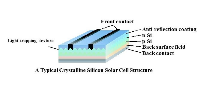
Solar Cell
| Material | Application | Instrument |
|---|---|---|
| Crystalline Silicon Solar Cell | Impurity analysis Defect photoluminescence |
FTIR PL |
| Silicon Based Thin Film Solar Cell | Hydrogen bond condition Crystallinity / Stress / Crystallite size |
FTIR Raman |
| CIGS Solar Cell | Transmittance and reflectance characteristics of transparent electrode, buffer layer, glass substrate | UV/Vis/NIR/IR |
| Dye Sensitized Solar Cell | Crystallization of semiconductor thin layer electrode Absorption band of dye sensitized element Structural analysis |
Raman UV/Vis/NIR/IR FTIR, Raman |
Up-conversion Phosphors Measuring System
Generally, the emission wavelength are longer than the excitation wavelength, appearing towards the red end of the wavelength range. Up-conversion phosphors, however, are significant because the emission wavelength is shorter than the excitation wavelength shifting towards the blue wavelengths. Recently, up-conversion technique has attracted much attention in the field of research and development of solar cell materials. JASCO has developed the evaluation system using the FP-8600 with the dedicated accessory mount for a 980 nm NIR laser. The figure shows the emission spectrum of the up-conversion phospor excited at 980 nm. Several peaks were observed in the visible region.
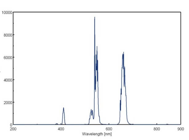
Emission Spectrum of Up-conversion Phosphor
Human eyes cannot detect the light of the 980 nm laser, but while the up-conversion phosphor is illuminated with this laser, the irradiated sample area can be observed as a green spot. This phenomenon can be explained as the luminescence from the up-conversion phosphor when it was excited by the 980 nm laser which products emission in the visible range.
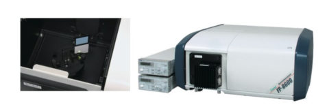
Up-conversion Phosphor Measuring System
Evaluation of Crystallinity of Si for Solar Cell
The peak of monocrystal Silicon spectrum shifts to lower wavenumber side as crystallinity of Silicon becomes less with peak shape broader. Distribution of crystallinity was evaluated by peak position and half width in XY mapping measurement of surface of Polycrystalline Silicon.
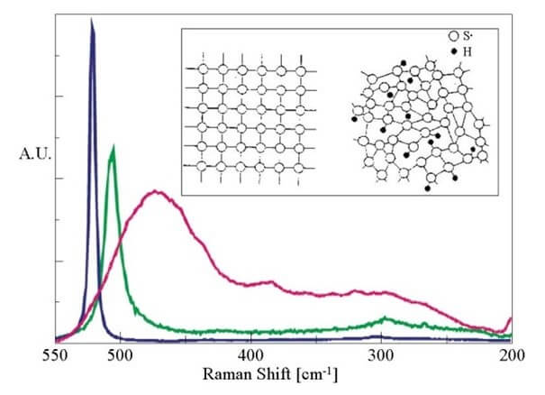
Si Peak Shift due to Crystallinity
Raman Imaging Microscopy
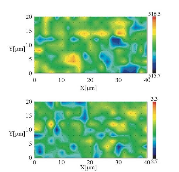
Crystallinity Image of Polycrystalline Silicon on Glass Substrate
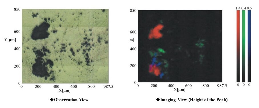
Complex Impurities on Silicon Wafer
Impurities on Silicon wafer were measured by high speed imaging and color coded image was created with peak height and PCA mapping analysis. Complex impurities including Protein, Cellulose and Calcium Carbonate were spatially separated and analyzed by using of high spatial resolution linear array detector and high speed imaging.
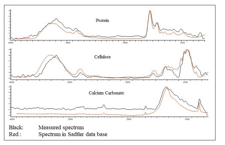
Sadler Library Search Result of Each Component
FTIR Imaging Microscopy
Related Posts:
 Base Material and Dye Analysis - Combined Raman and…
 Highly efficient spectral measurement methods using…
 Development and Applications of Full-Vacuum FT-IR…
 Stability Evaluation of Trastuzumab and Rituximab…
 Analysis of pollen collected by Durham sampler…
 Higher Order Structure, Stability, and Similarity…