Introduction
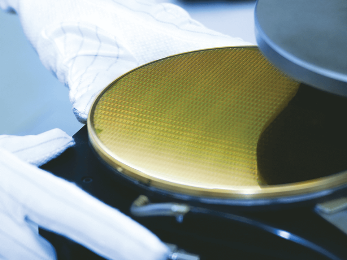
The Auto Y-theta stage, which can be mounted to the sample compartment of the FT/IR-4000/6000 series, enables to perform the transmittance/reflectance measurement of wafer sample up to 12 inches. This wafer measurement system is powerful tool for thickness measurement and impurity evaluation of Si wafer.
■ Features
● Non-destructive and non-contact measurement by using infrared spectrometry
● High precision and reproducibility
● Various measurements are available by collaborated with optional program “Concentration quantitative program in Si”
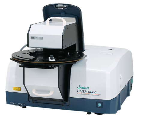
■ AYT12-4000 12-inch Wafer Auto Y-theta Stage
Enabled instruments: FT/IR-4000/6000 series
Method: transmission/reflection measurement (Center of incident angle: 15°)
Movable range: Y direction: 0 – 168 mm, Theta direction: -180 – 180 degree
Position accuracy: Y direction: ±0.5 mm, Theta direction: ±0.19 degree
Purge: Available
Software: Y-theta mapping measurement program
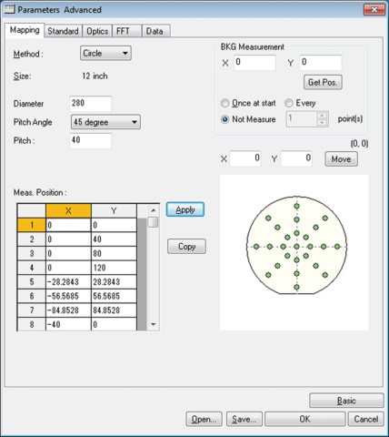
● Mapping measurement setting dialog
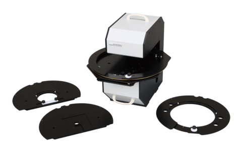
● Attachments corresponded to various sample size (option)
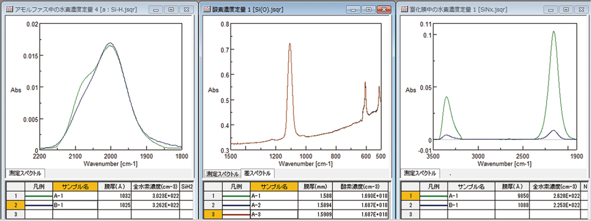
● Concentration quantitative program in Si (option)
These programs can perform impurity quantitative analysis which correspond to the following various standards uder JEITA regulation.
– Carbon concentration in Si: JEITA-EM-3503
– Oxygen concentration in Si: JEITA-61-2000
– Nitrogen concentration in Si: JEITA-EM-3512
– Hydrogen concentration in amorphous Si
– Hydrogen concentration in SiN film
* A vertical incident option for auto Y-theta stage is required.
* JEITA: Japan Electronics and Information Technology Industries Association

 properties of platinum complexes using a CPL measurement system and a spectrofluorometer")


")
")