Introduction
JASCO can provide the microscopic spectrophotometer, which is for transmission/reflection measurement in a wide wavelength range from ultraviolet to near-infrared. It allows the measurement of the area of as small as 10 µmφ and the built-in high resolution camera enables to observe the samples precisely to determine the area to be measured. This instrument is most suitable to measure the minute samples or samples having microstructure. This time, the sample on which Si patterns of 35 µm widths are lined up on Ti substrate with 14 µm intervals was measured as a microstructure sample. Actually, the thickness of SiO2 formed upon Si was analyzed from the obtained reflectance spectrum, because Si is easily oxidized in the air to form thin oxide film of SiO2.
MSV-5500 UV/VIS microscopic spectrophotometer
Experimental
Sample
Si and Si oxide film on the Ti substrate
Measurement
(1) Baseline: Al vapor-deposited mirror as a reference was used for baseline measurement.
(2) Measurement area: The sample was observed by the high resolution camera to determine the measurement area (Figure 1). The red spot in Figure 1 shows the size and position of detected light.
(3) Sample measurement: The reflectance spectrum was measured.
(4) Transforming into absolute reflectance: The absolute reflectance spectrum of the sample was calculated by multiplying the obtained relative reflectance by the absolute reflectance of Al vapor-deposited mirror.
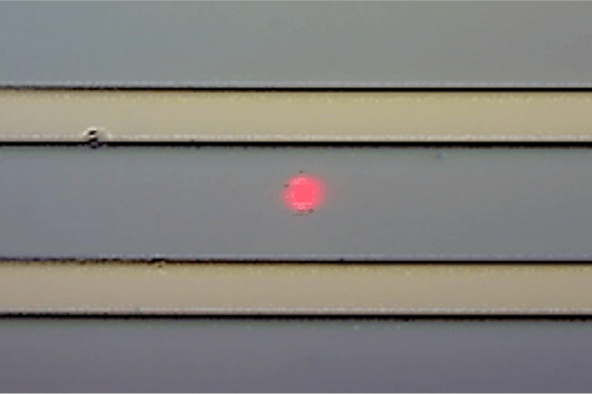
Figure 1. Observation figure of measurement position
Analysis
Reflectance (R) was expressed by the equation of refractive index of the film (ni), extinction coefficient (ki), the angle of incidence (qi), wavelength (l) and the film thickness (di). This time, optical constants of Si and SiO2 were used from the literature value. and then the film thickness of SiO2 was estimated by using [Multi-Layer Analysis] program by fitting the calculated reflectance spectrum to the measured one to make the thickness value reasonable.
Measurement parameters
UV/Vis spectral bandwidth: 5.0 nm
NIR spectral bandwidth: 20.0 nm
Scan speed: 100 nm/min
Response: Slow
Data interval: 0.5 nm
Cassegrain objective mirror: 16×
Incidence angle: 23 degrees
IN aperture: 10 µmφ
OUT aperture: 10 µmφ
Keywords
microscope, silicon, absolute reflectance
Results
Measured absolute reflectance spectrum is shown in Figure 2.
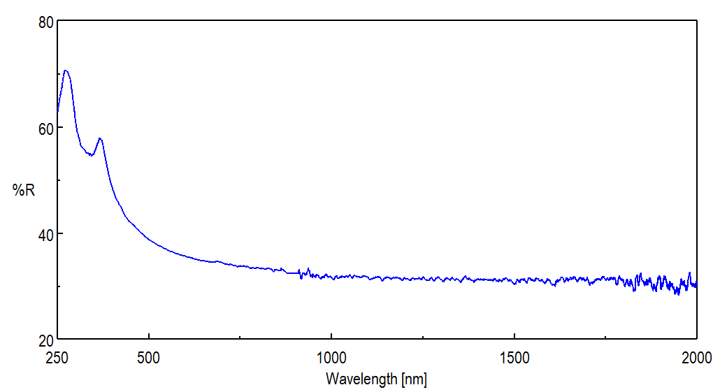
Figure 2. Absolute reflectance spectrum of sample
Since the confocal optical system is adopted, it is possible to perform the measurement eliminating the influence of back side reflection. In the range over 1100 nm where the light passes through Si, the spectrum would not be influenced by the back side reflection.
The result of fitting the reflectance spectra using [Multi-Layer Analysis] program is shown in Figure 3.
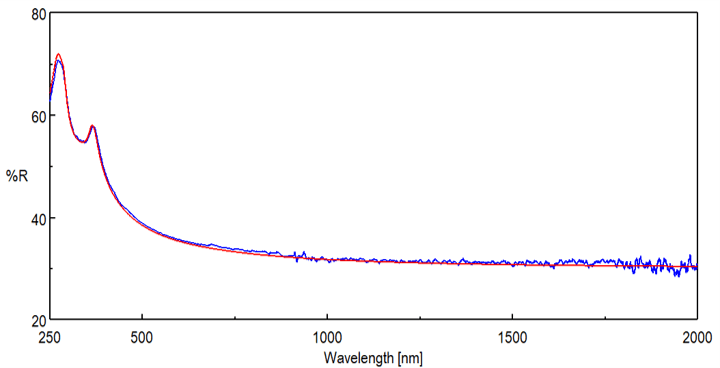
Figure 3. Fitting result of reflectance spectra
The error between measured spectrum and calculated one was within 2 % (Figure 4) and the film thickness of SiO2 was calculated to be 7.6 nm.
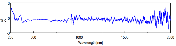
Figure 4. The error between measured spectrum and calculated one
Related Posts:
 Spectroscopic Evaluation of Color Development in…
 Vibrational Circular Dichroism Spectrometer based on…
 Evaluation of Reflectance of Microlens Surface using…
 Analysis of pollen collected by Durham sampler…
 Base Material and Dye Analysis - Combined Raman and…
 Combined Analysis of Thermochromic Materials -FT-IR…