Application of ultraviolet-visible microspectroscopy
Figure 1 shows an example of analysis using an ultraviolet-visible microspectroscopy system. It shows a microscopic image (right) and a transmission spectrum (left) of a color filter in a LCD panel. Ultraviolet-visible microspectroscopy allows the absorption spectrum for different pixels (RGB) in the microscopic image to be obtained. From the spectra you can see the regions where the light covers and those regions can be used to create a map of the sample.

Figure 1. Transmission spectrum of color filter on LCD panel (left) and microscopic image (right)
Application of infrared and Raman imaging
Figure 2 is an example comparing infrared and Raman imaging results. It shows optical, infrared, and Raman images of a cross section of a multilayer-film sample. Additionally, infrared and Raman principal component analysis spectra can be calculated by multivariate curve resolution (MCR) analysis. From the chemical images and the principal component analysis spectra, the distribution of polypropylene (PP), polyethylene (PE), and polyethylene terephthalate (PET) can be visualized. Some of the components appear in only either Raman or infrared. Cellulose, which is a highly infrared-active molecule, was detected only by infrared microscopy. Since cellulose was not deliberately included in this film, it can be assumed that it is a contaminant. Titanium oxide (TiO2) was detected only by Raman microscopy as an ultrathin layer with a thickness of several micrometers.. Thus, complementary information can be obtained by combining the two spectroscopic measurement methods.
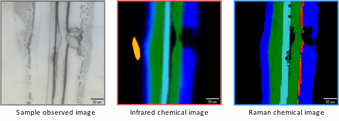
Figure 2. Comparison of infrared and Raman imaging results
Cutting-edge microscopic observations
Taking a quality image using a CCD camera requires tuning the brightness to best match the camera’s specifications. Since each objective collects a different amount of light, when the objective is changed, the light intensity should change. Automatically changing the objective and light intensity can produce high-resolution images. An example of high-resolution imaging of a semiconductor device using a Raman microspectrometer is shown in Figure 3. While analyzing foreign matter on the semiconductor surface, the objective lens was automatically switched and the observed image was enlarged. A clear microscope image could be obtained by adjusting the light intensity by automatic brightness correction.
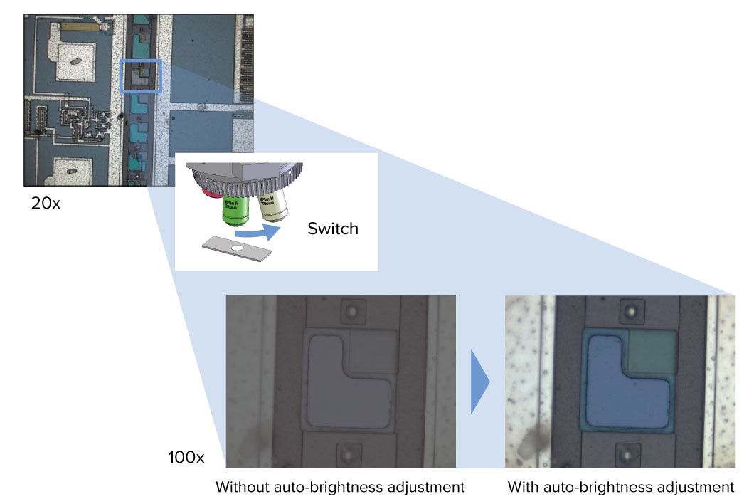
Figure 3. Enlarged field of view in Raman imaging
Another feature of JASCO’s Raman imaging is the possibility of analyzing rough samples automatically. Figure 4 shows 3D imaging results for rust on a metal surface. An omnifocal image could be obtained by a combination of scanning in the depth direction and high-speed imaging. Special software automatically recognizes where the image is in focus and combines the in focus portions of the images together to form a three dimensional image of the surface.
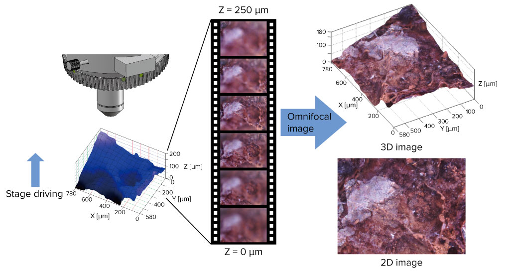
Figure 4. 3D Raman imaging of metal surface rust


