Introduction
Raman spectroscopy is widely used for evaluating chemical composition, orientation, crystallization, density, stress, temperature of semiconductor materials, and also for various structure-property evaluation such as impurity concentration, defect of semiconductor materials and composition ratio of mixed crystal semiconductor. Hall effect measurement with formed electrode is applied for evaluating electrical characteristics of carrier density in general, while Raman spectroscopy is also utilized for estimating carrier density of group III-V semiconductor. In this application data, we would like to show several measurement results using monocrystal SiC by Raman spectroscopy, such as determination of polymorphism and calculation of carrier density.
Laser Raman Spectrometer NRS-5500
Experimental
Evaluating crystal polymorphism
1: Background
It is well known that SiC crystal has more than 200 different types of polymorphism depending on atomic arrangement and these each polymorphism has different physical property. Among such many types of polymorphism, there are the most valuable ones starting from 4H polymorphism which has the biggest band gap and also high mobility and the trials have been attempted to grow crystals selectively as one of hot topics and challenge in field. Raman spectroscopy can evaluate and determine the type of polymorphism by analysis of peak patterns due to lattice vibration of crystals, appearing in low wavenumber region where the measurement is quite difficult by IR spectroscopy.
2: Experimental and result
Two kinds of SiC monocrystal with 0.33 mm thickness that have been prepared by vacuum sublimation method under the different conditions have been measured with 532 nm excitation and backscattering position. As the result of this experiment, by comparing measured spectra in the range of 150-200 cm-1 and 700- 800cm-1 with reference spectra in published paper1), two samples were determined to be 6H and 4H polymorphism respectively.
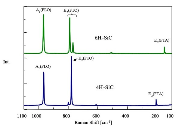
Fig. 1 Raman Spectra of 6H-SiC and 4H-SiC
Evaluating carrier density
1: Background
In manufacturing process of semiconductor materials, it is not unusual to dope some impurity material to pure semiconductor to increase the concentration of free election and electron hole as carrier. Regarding n-type compound semiconductor, Raman spectroscopy is applied as an easy method to estimate the carrier density.
In polar semiconductor such as GaN, GaAs, SiC, longitudinal wave and transverse wave due to lattice vibration of crystal can be observed separately in Raman spectra. Collective oscillation of free electron which exists in n-type semiconductor as carrier is called as Plasmon, which is longitudinal wave similar to sound wave. This plasma oscillation is the same kind of wave as the longitudinal wave due to lattice vibration, LO phonon and therefore they interact with each other. This interaction is magnified due to the concentration of carrier and this relevancy makes peak position of longitudinal wave due to lattice vibration shift to higher wavenumber side. Such peak shift is named as L+ and L– and shown in Fig. 2. In evaluation of SiC, only the peak of L+ can be observed by using of Raman spectroscopy. It is known that this peak shifts to higher wavenumber side with broadening peak shape when carrier concentration is increased, and accordingly, the absolute carrier concentration is evaluated by the peak position.
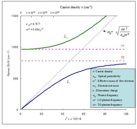
Fig. 2 Carrier concentration change vs. wavenumber shift ( L+ and L-) in combined mode of Plasmon and phonon
Fig. 2 shows that the energy level of Plasma oscillation, collective oscillation of free electron in semiconductor increases with increase of carrier concentration in compound semiconductor. Peak is shifted through interaction between LO phonon, longitudinal wave due to lattice vibration and Plasmon by resonance phenomenon which is generated under the condition that plasma frequency is close to the energy of lattice vibration. However, any peak shift cannot be observed for TO phonon, since TO photon, transverse wave due to lattice vibration does not have any such interaction.
2: Experimental and result
Samples in this experiment are 3 kinds of 4H-SiC monocrystal which have been grown to 0.33 mm thickness by several different conditioned sublimation method. Each sample is measured using JASCO NRS-5100 Raman Spectrometer with 532 nm excitation and backscattering position.
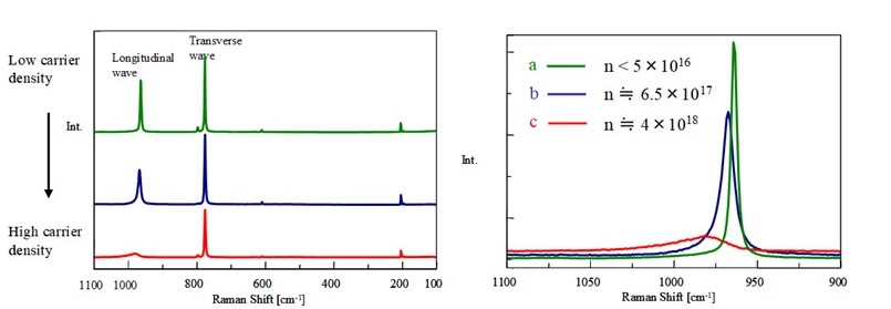
Fig. 3 Change of Raman spectrum of 4H-SiC due to carrier concentration(L), zoomed one (R)
Fig. 3 shows that peak wavenumber of longitudinal wave is different for each sample. The absolute carrier concentration can be estimated by inputting central wavenumber of each peak to theoretical curve which indicates the relationship between carrier concentration and LO phonon – Plasmon connection mode as shown in Fig. 4.
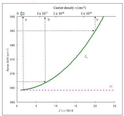
Fig. 4 Carrier concentration calculation from central wavenumber
References
Reference
1) S. Nakashima, and H. Harima, Phys . Stat . Sol . (a) 162, 39 (1997).
2) H. Harima, S. Nakashima, and T. Uemura, J . Appl . Phys ., 78, 1996 (1995).
Samples in this evaluation had been provided from Prf. Inushima and Mr. Ohta of Course of Electrical and Electronic System in Tokai University.


